MIC2584/2585
Micrel
MIC2584/2585
20
March 2005
2) Next, determine R12 using the output
good
voltage of 10.5V and the following equation:
V
V
R12 R13
R13
OUT1(Good)
FB1(MAX)
=
+
(
)
?/DIV>
?/DIV>
?/DIV>
?/DIV>
?/DIV>
?/DIV>
(10)
Using some basic algebra and simplifying Equation 10 to
isolate R12, yields:
R12 R13
V
V
1
OUT1(Good)
FB1(MAX)
=
?/DIV>
?/DIV>
?/DIV>
?/DIV>
?/DIV>
?/DIV>
?/DIV>
?/DIV>
?/DIV>
?/DIV>
?/DIV>
?/DIV>

?/DIV>
?/DIV>
(10.1)
where V
FB1(MAX)
= 1.29V, V
OUT1(Good)
= 10.5V, and R13 is
14.7k&. Substituting these values into Equation 10.1 now
yields R12 = 104.95k&. A standard 105k& ?1% is selected.
Now, consider the 11.4V minimum output voltage, the lower
tolerance for R13 and higher tolerance for R12, 14.55k& and
106.05k&, respectively. With only 11.4V available, the voltage
sensed at the FB1 pin exceeds V
FB1(MAX)
, thus the /POR and
PG1 (MIC2585) signals will transition from LOW to HIGH,
indicating
power is good
given the worse case tolerances of
this example. A similar approach should be used for Channel 2.
Output Undervoltage Detection
For output undervoltage detection, the first consideration is to
establish the output voltage level that indicates
power is
good.
For this example, the output value for which a 12V
supply will signal
good
is 10.5V. Next, consider the toler-
ances of the input supply and FB threshold (V
FB
). For this
example, given a 12V ?% supply for Channel 1, the resulting
output voltage may be as low as 11.4V and as high as 12.6V.
Additionally, the FB1 threshold has ?0mV tolerance and
may be as low as 1.19V and as high as 1.29V. Thus, to
determine the values of the resistive divider network (R12
and R13) at the FB1 pin, shown in the typical application
circuit on page 1, use the following iterative design proce-
dure.
1) Choose R13 so as to limit the current through
the divider to approximately 100礎 or less.
R13
V
100 A
1.29V
100 A
12.9k
FB1(MAX)
E
?/DIV>
E
?/DIV>
E
&
.
R13 is chosen as 14.7k& ?1%.
C6
0.1礔
R1
33k&
R2
47k&
SENSE1
VCC1
R
SENSE1
0.012&
5%
1
2
3
4
24
23
SENSE2
VCC2
R
SENSE2
0.012&
5%
1
2
3
4
1
2
C4
0.022礔
Q2
IRF7822
(SO-8)
C
LOAD1
220礔
V
OUT1
5V@2.5A
V
OUT2
3.3V@2.5A
C
LOAD2
220礔
C3
0.022礔
C7
0.033礔
Q4
TCR22-4
Q3
ZTX788A
Q1
IRF7822
(SO-8)
GND
TRK
3
5
6
7
22
20
18
13
9
GATE2
OUT2
DIS2
19
DIS1
OUT1
FB2
FB1
GATE1
CDLY
12
CFILTER
11
ON
8
Undervoltage (OUT1) = 4.4V
Undervoltage (OUT2) = 2.85V
Circuit Breaker Response Time = 5ms
Sequenced Output Delay (Turn-On) = 20ms
*Dual package Diode is AZ23C8V2
Resistors are 5% unless specified otherwise
Additional pins omitted for clarity
C5
0.01礔
C2
1礔
R6
8.66k&
1%
R7
680&
R8
1.5k&
R10
360&
R9
3.6k&
R3
39.2k&
1%
R4
15.8k&
1%
R5
20.5k&
1%
*D1
(8V)
*D2
(8V)
C1
1礔
MIC2585-1
V
IN1
5V
V
IN2
3.3V
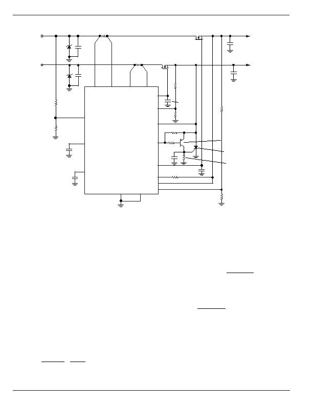
Figure 8. First OnLast Off Application Circuit
发布紧急采购,3分钟左右您将得到回复。
相关PDF资料
MIC2586R-2BM TR
IC CTRLR/SEQ HOT SWAP 14-SOIC
MIC2587R-2BM TR
IC CTRLR HOT SWAP POS HV 8-SOIC
MIC2590B-5BTQ TR
IC PCI HOT PLUG CTLR DUAL 48TQFP
MIC2591B-2BTQ TR
IC PCI HOT PLUG CTLR DUAL 48TQFP
MIC2592B-2BTQ TR
IC PCI HOT PLUG CTLR DUAL 48TQFP
MIC2593-2BTQ TR
IC PCI HOT PLUG CTLR DUAL 48TQFP
MIC2594-2BM TR
IC CTRLR HOT SWAP NEG HV 8-SOIC
MIC2595R-2BM TR
IC CTRLR HOT SWAP NEG HV 14-SOIC
相关代理商/技术参数
MIC2586-1BM
功能描述:IC CTRLR/SEQ HOT SWAP 14-SOIC RoHS:否 类别:集成电路 (IC) >> PMIC - 热交换 系列:- 产品培训模块:Obsolescence Mitigation Program 标准包装:100 系列:- 类型:热插拔开关 应用:通用 内部开关:是 电流限制:可调 电源电压:9 V ~ 13.2 V 工作温度:-40°C ~ 150°C 安装类型:表面贴装 封装/外壳:10-WFDFN 裸露焊盘 供应商设备封装:10-TDFN-EP(3x3) 包装:管件
MIC2586-1BM TR
功能描述:IC CTRLR/SEQ HOT SWAP 14-SOIC RoHS:否 类别:集成电路 (IC) >> PMIC - 热交换 系列:- 产品培训模块:Obsolescence Mitigation Program 标准包装:100 系列:- 类型:热插拔开关 应用:通用 内部开关:是 电流限制:可调 电源电压:9 V ~ 13.2 V 工作温度:-40°C ~ 150°C 安装类型:表面贴装 封装/外壳:10-WFDFN 裸露焊盘 供应商设备封装:10-TDFN-EP(3x3) 包装:管件
MIC2586-1YM
功能描述:热插拔功率分布 Positive High Voltage Hot-Swap Controller/Sequencer - Lead Free
RoHS:否 制造商:Texas Instruments 产品:Controllers & Switches 电流限制: 电源电压-最大:7 V 电源电压-最小:- 0.3 V 工作温度范围: 功率耗散: 安装风格:SMD/SMT 封装 / 箱体:MSOP-8 封装:Tube
MIC2586-1YM TR
功能描述:热插拔功率分布 Positive High Voltage Hot-Swap Controller/Sequencer - Lead Free
RoHS:否 制造商:Texas Instruments 产品:Controllers & Switches 电流限制: 电源电压-最大:7 V 电源电压-最小:- 0.3 V 工作温度范围: 功率耗散: 安装风格:SMD/SMT 封装 / 箱体:MSOP-8 封装:Tube
MIC2586-2BM
功能描述:IC CTRLR/SEQUENCE HOTSWAP 14SOIC RoHS:否 类别:集成电路 (IC) >> PMIC - 热交换 系列:- 产品培训模块:Obsolescence Mitigation Program 标准包装:100 系列:- 类型:热插拔开关 应用:通用 内部开关:是 电流限制:可调 电源电压:9 V ~ 13.2 V 工作温度:-40°C ~ 150°C 安装类型:表面贴装 封装/外壳:10-WFDFN 裸露焊盘 供应商设备封装:10-TDFN-EP(3x3) 包装:管件
MIC2586-2BM TR
功能描述:IC CTRLR/SEQ HOT SWAP 14-SOIC RoHS:否 类别:集成电路 (IC) >> PMIC - 热交换 系列:- 产品培训模块:Obsolescence Mitigation Program 标准包装:100 系列:- 类型:热插拔开关 应用:通用 内部开关:是 电流限制:可调 电源电压:9 V ~ 13.2 V 工作温度:-40°C ~ 150°C 安装类型:表面贴装 封装/外壳:10-WFDFN 裸露焊盘 供应商设备封装:10-TDFN-EP(3x3) 包装:管件
MIC2586-2YM
功能描述:热插拔功率分布 Positive High Voltage Hot-Swap Controller/Sequencer - Lead Free
RoHS:否 制造商:Texas Instruments 产品:Controllers & Switches 电流限制: 电源电压-最大:7 V 电源电压-最小:- 0.3 V 工作温度范围: 功率耗散: 安装风格:SMD/SMT 封装 / 箱体:MSOP-8 封装:Tube
MIC2586-2YM TR
功能描述:热插拔功率分布 Positive High Voltage Hot-Swap Controller/Sequencer - Lead Free
RoHS:否 制造商:Texas Instruments 产品:Controllers & Switches 电流限制: 电源电压-最大:7 V 电源电压-最小:- 0.3 V 工作温度范围: 功率耗散: 安装风格:SMD/SMT 封装 / 箱体:MSOP-8 封装:Tube
